Product Summary
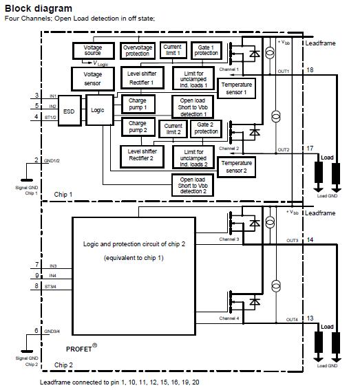
The bts712n1 is an N channel vertical power FET with charge pump, ground referenced CMOS compatible input and diagnostic feedback, monolithically integrated in Smart SIPMOS technology. The device can provide embedded protective functions. Applications of the bts712n1 include μC compatible power switch with diagnostic feedback for 12 V and 24 V DC grounded loads, All types of resistive, inductive and capacitive loads and Replaces electromechanical relays and discrete circuits.
Parametrics
bts712n1 absolute maximum ratings: (1)Supply voltage (overvoltage protection), Vbb: 43 V; (2)Supply voltage for full short circuit protection Tj,start =-40 to+150℃, Vbb: 34 V; (3)Load current (Short-circuit current), IL: self-limited; (4)Load dump protection VLoadDump = UA + Vs, UA = 13.5 V RI = 2 Ω, td = 200 ms; IN= low or high, each channel loaded with RL = 7.1Ω, VLoad dump: 60 V; (5)Operating temperature range, Tj: -40 to +150℃; (6)Storage temperature range, Tstg: -55 to +150℃; (7)Power dissipation (DC) (all channels active), Ptot: 3.6W when Ta = 25℃; 1.9W when Ta = 85℃; (8)Inductive load switch-off energy dissipation, single pulse Vbb =12V, Tj,start =150℃, EAS: 150mJ when IL = 1.9 A, ZL = 66 mH, 0Ω one channel; 320mJ when IL = 2.8 A, ZL = 66 mH, 0Ω two parallel channels; 800mJ when IL = 4.4 A, ZL = 66 mH, 0Ω four parallel channels; (9)Electrostatic discharge capability (ESD) (Human Body Model), VESD: 1.0 kV; (10)Input voltage (DC), VIN: -10 to +16 V; (11)Current through input pin (DC), IIN: ±2.0mA; (12)Current through status pin (DC), IST: ±5.0mA; (13)junction - soldering point each channel, Rthjs: 16 K/W; (14)junction - ambient5 one channel active, Rthja: 44 K/W; all channels active: 35 K/W.
Features
bts712n1 absolute maximum ratings: (1)Supply voltage (overvoltage protection), Vbb: 43 V; (2)Supply voltage for full short circuit protection Tj,start =-40 to+150℃, Vbb: 34 V; (3)Load current (Short-circuit current), IL: self-limited; (4)Load dump protection VLoadDump = UA + Vs, UA = 13.5 V RI = 2 Ω, td = 200 ms; IN= low or high, each channel loaded with RL = 7.1Ω, VLoad dump: 60 V; (5)Operating temperature range, Tj: -40 to +150℃; (6)Storage temperature range, Tstg: -55 to +150℃; (7)Power dissipation (DC) (all channels active), Ptot: 3.6W when Ta = 25℃; 1.9W when Ta = 85℃; (8)Inductive load switch-off energy dissipation, single pulse Vbb =12V, Tj,start =150℃, EAS: 150mJ when IL = 1.9 A, ZL = 66 mH, 0Ω one channel; 320mJ when IL = 2.8 A, ZL = 66 mH, 0Ω two parallel channels; 800mJ when IL = 4.4 A, ZL = 66 mH, 0Ω four parallel channels; (9)Electrostatic discharge capability (ESD) (Human Body Model), VESD: 1.0 kV; (10)Input voltage (DC), VIN: -10 to +16 V; (11)Current through input pin (DC), IIN: ±2.0mA; (12)Current through status pin (DC), IST: ±5.0mA; (13)junction - soldering point each channel, Rthjs: 16 K/W; (14)junction - ambient5 one channel active, Rthja: 44 K/W; all channels active: 35 K/W.
Diagrams

| Image | Part No | Mfg | Description |  |
Pricing (USD) |
Quantity | ||||||||||||
|---|---|---|---|---|---|---|---|---|---|---|---|---|---|---|---|---|---|---|
 |
 BTS712N1 |
 Infineon Technologies |
 Power Switch ICs - POE / LAN SMART 4-CH HI-SIDE PWR SWITCH |
 Data Sheet |

|
|
||||||||||||
| Image | Part No | Mfg | Description |  |
Pricing (USD) |
Quantity | ||||||||||||
 |
 BTS707 |
 Infineon Technologies |
 Power Switch ICs - POE / LAN PROFET SMART 2 CH Hi Side Pwr SW |
 Data Sheet |

|
|
||||||||||||
 |
 BTS710L1 |
 Other |
 |
 Data Sheet |
 Negotiable |
|
||||||||||||
 |
 BTS711L1 |
 Infineon Technologies |
 Power Switch ICs - Power Distribution SMART 4-CH HI-SIDE PWR SWITCH |
 Data Sheet |

|
|
||||||||||||
 |
 BTS712N1 |
 Infineon Technologies |
 Power Switch ICs - POE / LAN SMART 4-CH HI-SIDE PWR SWITCH |
 Data Sheet |

|
|
||||||||||||
 |
 BTS716G |
 Infineon Technologies |
 Power Switch ICs - POE / LAN Smart High Side PROFET Quad |
 Data Sheet |

|
|
||||||||||||
 |
 BTS716GB |
 Infineon Technologies |
 Power Switch ICs - POE / LAN SMART HI SIDE PWR SWITCH INDUSTRY APP |
 Data Sheet |

|
|
||||||||||||
 (China (Mainland))


